Discover Premium Ceramic Products | Durability & Elegance United | Advanced Ceramics
PRODUCT PARAMETERS
Description
Overview of Boron Nitride Ceramic
Boron Nitride (BN) ceramic is a unique material renowned for its exceptional properties, making it highly valuable in various industrial applications. It exists in multiple forms, primarily hexagonal boron nitride (h-BN), cubic boron nitride (c-BN), and wurtzite boron nitride (w-BN). Hexagonal BN, the most common form, is often compared to graphite due to its lubricious and thermally conductive yet electrically insulating nature. Boron Nitride ceramics are synthesized under high temperatures and pressures, offering a rare combination of properties not found in many other materials.
Features of Boron Nitride Ceramic
Thermal Conductivity: Excellent thermal conductivity, especially in the hexagonal form, allowing efficient heat dissipation.
Electrical Insulation: Outstanding electrical insulation properties make it ideal for electrical applications requiring thermal management.
Chemical Stability: Highly resistant to chemical attacks, including strong acids and bases, ensuring durability in harsh environments.
Thermal Shock Resistance: Superior resistance to thermal shock, enabling it to withstand rapid temperature changes without cracking.
Mechanical Strength: Good mechanical strength at both room and elevated temperatures, although this can vary with the form of BN.
Lubricity: Self-lubricating property due to its layered structure, which reduces friction and wear in moving parts.
Non-Toxic: Safe to use in various settings, including medical and food processing industries, due to its non-toxic nature.
High-Temperature Performance: Maintains stability at extremely high temperatures, exceeding 1000°C in inert atmospheres, making it suitable for refractory applications.
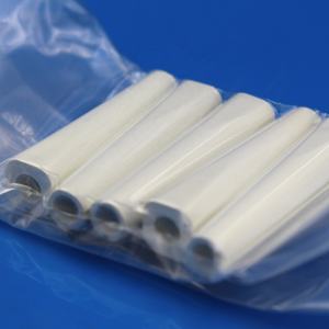
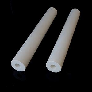
(High Purity Pyrolytic Boron Nitride (PBN) Thin Ceramic Sheet Plate for Semiconductor Processing Cut to Size)
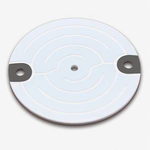
Specification of High Purity Pyrolytic Boron Nitride (PBN) Thin Ceramic Sheet Plate for Semiconductor Processing Cut to Size
High Pureness Pyrolytic Boron Nitride (PBN) Thin Ceramic Sheet Plates are designed for innovative semiconductor handling. These plates are made via chemical vapor deposition, making sure high pureness degrees above 99.99%. This purity decreases contamination threats in sensitive semiconductor atmospheres. The product framework is extremely purchased, offering outstanding thermal and chemical security.
PBN sheets handle severe temperature levels, with a maximum operating temperature level of 2000 ° C in inert atmospheres. They stand up to thermal shock, preserving integrity throughout rapid temperature modifications. This makes them ideal for high-temperature processes like epitaxial growth and crystal manufacturing.
The product uses outstanding electrical insulation. Its dielectric strength avoids existing leakage in semiconductor tools. PBN’s reduced dielectric continuous and loss variable boost efficiency in high-frequency applications. This is critical for components in digital circuits and shielding parts.
Mechanical residential or commercial properties consist of high rigidity and low weight. The thickness ranges from 2.0 to 2.2 g/cm FIVE, ensuring longevity without adding bulk. Flexural toughness goes beyond 100 MPa, standing up to contortion under tension. Surface area firmness approaches alumina, reducing wear throughout handling.
Chemical inertness is a vital advantage. PBN withstands rust from acids, antacid, and molten steels. This makes certain long-term dependability in aggressive processing atmospheres. The product does not react with the majority of semiconductor forerunners, protecting process honesty.
Modification is available. Sheets are reduced to dimension, with densities from 0.1 mm to 5 mm. Criterion dimensions consist of 100 mm x 100 mm to 300 mm x 300 mm. Bigger dimensions or particular forms can be generated on demand. Surface area surfaces are customized to application demands, from as-deposited to brightened.
Applications cover semiconductor manufacturing. PBN sheets work as crucibles for melting gallium arsenide or silicon. They work as substratums for depositing thin movies or growing single crystals. Shielding parts in activators and heaters gain from their thermal properties. Diffusion barriers prevent contamination in high-purity processes.
These sheets are utilized in sectors like LED manufacturing, aerospace, and study laboratories. Compatibility with vacuum cleaner systems and plasma atmospheres guarantees adaptability. The material meets stringent sector criteria for pureness and performance.
Schedule includes quick turnaround for conventional sizes. Custom orders require minimal lead time. Technical support is attended to combination right into existing systems. Specs are confirmed through third-party testing, guaranteeing uniformity.
(High Purity Pyrolytic Boron Nitride (PBN) Thin Ceramic Sheet Plate for Semiconductor Processing Cut to Size)
Applications of High Purity Pyrolytic Boron Nitride (PBN) Thin Ceramic Sheet Plate for Semiconductor Processing Cut to Size
High purity pyrolytic boron nitride (PBN) slim ceramic sheet plates are vital in semiconductor processing. These sheets handle extreme heat and stand up to chemicals. They function well in high-temperature settings. Semiconductor manufacturers use PBN sheets for growing crystals and depositing slim movies. Their security guarantees very little contamination during manufacturing.
PBN sheets serve as crucibles in chemical vapor deposition (CVD). They hold products at heats without responding. This keeps the procedure pure. PBN likewise works in molecular light beam epitaxy (MBE) systems. It produces smooth surfaces for expanding semiconductor layers. The sheets avoid pollutants from getting in delicate materials.
The sheets are perfect for making components like heating systems and insulators. PBN withstands fast temperature adjustments. It remains secure under thermal tension. This reduces devices downtime. Semiconductor tools last much longer with PBN parts. Maintenance expenses drop.
PBN sheets are reduced to size for personalized applications. Factories utilize them as shields or liners in high-heat areas. They safeguard tools from corrosive gases. PBN serves as a barrier between responsive materials and device components. This prolongs the life of processing chambers.
The material is electrically insulating. It prevents current leak in semiconductor tools. PBN sheets different conductive components safely. They handle warmth in power electronic devices. This enhances gadget reliability.
PBN sheets match wafer handling and annealing. They prevent infecting silicon wafers. The sheets handle temperature levels over 2000 ° C. They stay intact in vacuum or inert gas atmospheres. This makes them suitable for advanced chip manufacturing.
Semiconductor labs select PBN for its purity. It has reduced levels of metals and oxygen. This meets stringent sector standards. PBN makes certain regular results in sensitive processes. Its efficiency sustains next-gen semiconductor growth.
Personalized sizing allows accurate combination right into tools. Slim PBN sheets adjust to limited spaces. They preserve structural toughness even in slim types. Manufacturers obtain tailored services for specific manufacturing needs.
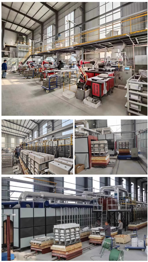
Company Introduction
Advanced Ceramics founded on October 17, 2014, is a high-tech enterprise committed to the research and development, production, processing, sales and technical services of ceramic relative materials and products.. Since its establishment in 2014, the company has been committed to providing customers with the best products and services, and has become a leader in the industry through continuous technological innovation and strict quality management.
Our products includes but not limited to Silicon carbide ceramic products, Boron Carbide Ceramic Products, Boron Nitride Ceramic Products, Silicon Carbide Ceramic Products, Silicon Nitride Ceramic Products, Zirconium Dioxide Ceramic Products, Quartz Products, etc. Please feel free to contact us.(nanotrun@yahoo.com)
Payment Methods
T/T, Western Union, Paypal, Credit Card etc.
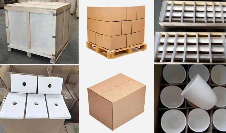
Shipment Methods
By air, by sea, by express, as customers request.
5 FAQs of High Purity Pyrolytic Boron Nitride (PBN) Thin Ceramic Sheet Plate for Semiconductor Processing Cut to Size
1. What is High Purity Pyrolytic Boron Nitride (PBN)?
PBN is a ceramic material made by heating boron and nitrogen gases at high temperatures. It forms thin sheets with strong heat resistance. It works well in high-temperature semiconductor processes. Its structure is layered, making it stable under extreme conditions. It resists chemical reactions, ideal for sensitive applications.
2. Why is PBN used in semiconductor processing?
Semiconductor manufacturing needs materials that handle heat without breaking down. PBN stays stable above 2000°C. It does not react with most chemicals. This prevents contamination in processes like crystal growth. Its purity ensures no unwanted particles affect semiconductor quality. It lasts longer than other materials under harsh conditions.
3. How pure is PBN?
PBN sheets have over 99.99% purity. Impurities like oxygen or carbon are below 10 parts per million. High purity is critical for semiconductors. Even tiny contaminants can ruin electronic components. The production process avoids additives, ensuring minimal foreign elements. This makes PBN reliable for advanced tech applications.
4. Can PBN sheets be cut to specific sizes?
Yes. PBN sheets are often customized for equipment. Laser cutting or diamond tools create precise shapes. Smooth edges prevent cracks or particles. Custom sizes fit reactors, crucibles, or insulation parts. Proper cutting avoids damaging the material’s structure. Suppliers typically offer cutting services based on user requirements.
5. How should PBN sheets be handled?
Avoid dropping or bending PBN sheets. They are brittle and can crack under force. Clean surfaces with solvents like alcohol before use. Store in dry areas to prevent moisture absorption. Do not expose to sudden temperature changes. Inspect regularly for chips or cracks. Replace damaged sheets to maintain process safety.
(High Purity Pyrolytic Boron Nitride (PBN) Thin Ceramic Sheet Plate for Semiconductor Processing Cut to Size)
REQUEST A QUOTE
RELATED PRODUCTS
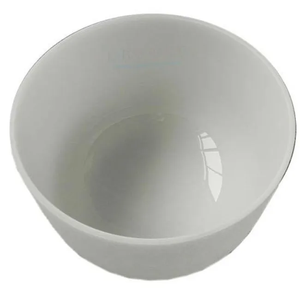
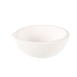
Hot Pressed BN Ceramic Crucible Vacuum 2000 Degrees Boron Nitride Ceramic Insulation Cup
High Purity BN Insulating Ceramic Plate Boron Nitride Sheet
Boron Nitride CAS 10043-11-5 Ceramic Coating Daily Chemicals Chinese Factory
High Purity BN Ceramic Boron Nitride Crucible for Melting
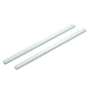
Low Density 99.99% Boron Nitride BN Ceramic Shaft Rod For Refractory Hot Pressed Insulation